
Graphene: Taking Electronics Beyond Silicon
When: Friday, October 28, at 8:30 a.m.
The Georgia Institute of Technology organized a one-day workshop on graphene, the ultra-thin carbon material that promises to advance electronics beyond silicon.
Leading French and American scientists in the field gave keynote presentations and shared ideas to nurture existing partnerships and foster new collaborations between US and French research institutions.
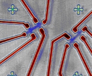
![]() Epitaxial Graphene as an Electronic Material
Epitaxial Graphene as an Electronic Material
Dr. Walt A. de Heer, Regents’ Professor, School of Physics, Georgia Institute of Technology, Atlanta
![]() Advances in Graphene Chemistry
Advances in Graphene Chemistry
Dr. Robert C Haddon, Distinguished Professor of Chemistry, and Chemical and Environtal Engineering, University of California, Riverside
![]() Synchrotron Opportunities for Surface Science in Graphene
Synchrotron Opportunities for Surface Science in Graphene
Dr. Amina Taleb-Ibrahimi, CNRS, Synchrotron Soleil
![]() Graphene and Spintronics
Graphene and Spintronics
Dr. Albert Fert, Nobel Prize 2007 in Physics, University Paris-Sud
![]() Carbon Based Optoelectronics
Carbon Based Optoelectronics
Dr. Bernard Kippelen, Professor; Director, Center for Organic Photonics and Electronics, Georgia Institute of Technology, Atlanta
![]() Overview of the Graphene Programs in France and Future European Projects
Overview of the Graphene Programs in France and Future European Projects
TBA
![]() NSF Funding Programs
NSF Funding Programs
Dr. David Stonner, NSF - Office of International Science and Engineering
Dr. Janice Hicks, NSF - Division of Materials Research
Dr. Thomas Rieker, NSF - Materials Research Centers and Teams
Seating limited.
Contacts : Jacqueline Signorini, Scientific Attaché, attache-univ.mst@ambascience-usa.org
For more information about France-USA scientific cooperation, see France-science.org
“Graphene Nanoribbons: New Technique Produces Structures with Metallic Properties and Sets Stage for New Generation of Quantum Devices”
A new “templated growth” technique for fabricating nanoribbons of epitaxial graphene has produced structures just 15 to 40 nanometers wide that conduct current with almost no resistance. These structures could address the challenge of connecting graphene devices made with conventional architectures – and set the stage for a new generation of devices that take advantage of the quantum properties of electrons.
_ “We can now make very narrow, conductive nanoribbons that have quantum ballistic properties,” said Walt de Heer, a professor in the School of Physics at the Georgia Institute of Technology. “These narrow ribbons become almost like a perfect metal. Electrons can move through them without scattering, just like they do in carbon nanotubes.”
De Heer discussed recent results of this graphene growth process March 21st at the American Physical Society’s March 2011 Meeting in Dallas.
“In our templated growth approach, we have essentially eliminated the edges that take away from the desirable properties of graphene,” de Heer explained. “The edges of the epitaxial graphene merge into the silicon carbide, producing properties that are really quite interesting.”
In creating these graphene nanostructures, de Heer and his research team first use conventional microelectronics techniques to etch tiny “steps” into a silicon carbide wafer whose surface has been made extremely flat. They then heat the contoured wafer to approximately 1,500 degrees Celsius, which initiates melting that polishes any rough edges left by the etching process.
To know more, click on the following link: Graphene Nanoribbons at Georgia Tech
With the support of: